| 5.4 | The charge indicator | previous |
| 5.4.1 | Introduction | index page |
For understanding the design demands for the charge indicator and the technical characteristics of the resulting design, one needs at least a basic knowledge of electricity and electronics and preferably also some experience with it. But for people who are not trained and experienced, it should be possible to build, test and calibrate charge indicators as long as a clear, step by step manual is available. That is what this chapter will try to provide.
People who are interested in why the charge indicator was designed this way and how it works, are encouraged to read annex D: More about Charge indicators. If technical problems arise that can not be solved which the help of par. 5.4.5, one will have to refer to annex D. Then it should be possible to work out what part of the indicator does not work as it should, and find a remedy for this.
There are clear `economies of scale' in building charge indicators. Learning how to build them, buying the components, getting the equipment that is needed and making the Printed Circuit Boards will take about as much time irrespective of whether one builds 5 or 100 pieces. Also the actual building, testing and calibrating will go much faster as one gets more experienced and builds some simple, handy devices. So from that point of view, it makes sense to buy indicators from abroad as long as only a limited number of indicators are needed (see par. 7.4), and not start building oneself. This saves a lot of time and also reduces the risc that the project will run into problems because one essential device as the indicator cannot be built locally yet. Then one could start producing indicators in a later stage, when a steady supply of indicators is needed since more chargers are built and installed. There is no clear number of indicators above which it becomes attractive to start producing them locally, this number depends on:
Then there is the possibility of having indicators built in a workshop in-country:
| 5.4.2 | How to avoid deep discharge of batteries |
The batteries are the single most expensive item in the investment costs of a firefly micro hydro scheme. In the operating costs, replacement costs of worn-out batteries will form the major part of the money that is spent outside the community itself (the charging fee is also a major expense, but this money remains in the community). Poor care for batteries and the resulting poor life span can lead to disappointing performance and operating costs being too high for poor potential users.
A main cause for premature battery failure is deep discharge (see par. 5.4.2). In a battery that is often discharged too deep or that has been left in discharged condition for a long time, the plates gradually get covered with a hard layer of lead sulphate which makes them ineffective. High temperatures and big changes in temperature promote this. This process is called sulphatizing and it makes a battery lose its capacity to store electricity (VAN DER MEER, 1990, see also annex C: Sulphatizing).
To reduce this effect to an acceptable level, normal car batteries should be discharged to only 50 % of its capacity (so: 50 % of its capacity should be left unused). Solar batteries are designed for `deep cycle' and can safely be discharged until 80 % (so: 20 % of capacity left unused).
However, users will be temped to use their battery too long:
In order to avoid deep discharge, users should be able to measure how far their battery is discharged. This is where the charge indicator comes in: It measures the state of charge of a battery (there are also other types of devices to measure state of charge or prevent deep discharge, see annex D.1: Strategy to prevent deep discharge).
Then the strategy for preventing deep discharge of batteries could be like this:
| 5.4.3 | Buying components |
Buying component is not as easy as it would be in western countries, especially when one tries to buy cheap. At least that was the experience in Manila. There are two problems:
First about the kind of shops where electronic components are sold:
Clearly suppliers to electronics workshops are not a safe choice in case one is not experienced enough to test the parts before buying. If the electronics hobbyist shops are not around and wholesalers are unwilling to accept small orders, the best answer is to look for assistence in buying the parts:
Both a small repair workshop and a larger production workshop might become useful contacts in the future when the development worker who started it all has gone and indicators should be produced locally. A list of all parts that are needed for the indicator is given in the next paragraph.
| 5.4.4 | Building the indicators |
| 5.4.4.1 | Electronic circuit and parts list |
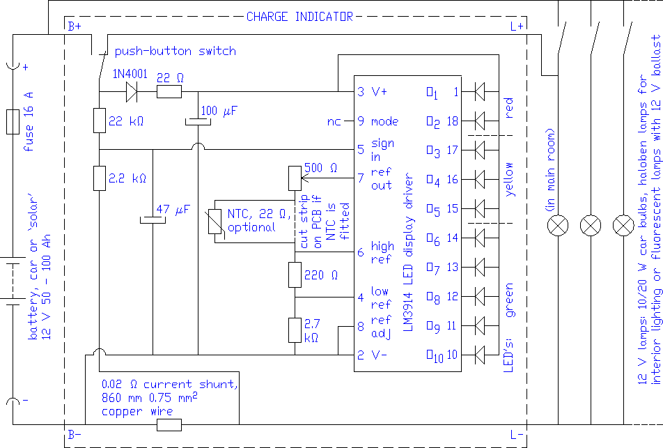
The electric circuit of the indicator is given in fig. 5.3.
It would go too far to explain in detail how the indicator circuit works, this is done in annex D: More about charge indicators. Also it is not necessary to understand this exactly as long as one is able to build, test, calibrate and install indicators correctly. All parts needed for the indicator are included in the parts list, see table 5.2.
|
| Fig. 5.3: Electrical circuit of home system |
| Part: | Value / type no / pcs needed: | Polarity: | Remarks: | ||
| Resistors: | indifferent | all 1/4 Watt, 5 % accuracy (last band has gold color), color code:. | |||
| R1 | 22 Ohm | red - red - black - gold | |||
| R2 | 22 kOhm | red - red - orange - gold | |||
| R3 | 2.2 kOhm | red - red - red - gold | |||
| R5 | 220 Ohm | red - red - brown - gold | |||
| R6 | 2.7 kOhm | red - violet - red - gold | |||
| If you are not sure: Measure resistance value with a tester | |||||
| Trimmer: | Connections are O.K. if it fits on the PCB. | Closed plastic model, miniature, upright version. The lying version or the standard size will not fit into the PCB. There are also cheaper trimmers consisting of a little piece of board with resistive material on it and the connections fixed to it. Such trimmers are undesirable because they are much more difficult to calibrate. | |||
| R4 | 500 Ohm | ||||
| Current shunt: | indifferent | Note: When using the PCB design with an
on-board current shunt of fig. 5.5b,
there is no need for a separate current shunt Made from 0.75 mm² massive copper wire. To give the right resistance, the length between the connections to the PCB should be 860 mm. At each end, it should extend ca. 40 mm so that these ends can be connected to the connector block, which makes total length ca. 940 mm. The switch and the connections of `B+' and `L+' from the PCB to the connector block can be made with the same type of wire, so for these some 150 mm more is needed. Copper wire with another cross-section can also be used as long as the resistance between the connections to the PCB is 0.02 Ohm. |
|||
| 0.02 Ohm | |||||
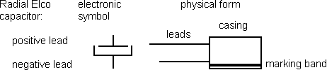
| Elco capacitors: | Negative lead is marked with a bold line1 | `Radial' version, with both leads coming out on one side, check whether the size fits onto the PCB. Capacitors with a higher voltage rating have a larger diameter and fit poorly on the PCB. | |||
| C1 | 100µF/16 V | ||||
| C2 | 47 µF/16 | ||||
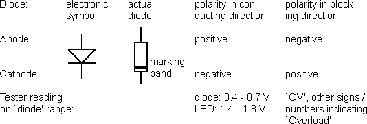
| Diode: | Cathode2 is marked with a band | Other low-voltage types will also do. The smallest types (e.g.1N4148) have too low a capacity and might eventually get destroyed. | |||
| D | 1N4001 | ||||
| Chip: | In the component lay-out of fig. 5.4, the marking notch must be at the left (where `1' is printed on copper side). | Usually the text on the chip (type no etc.) will end up upright. However, some chips could have their text upside down. So use the marking notch as reference. Often pin 1 is also marked with a `1' or a little pit. | |||
| LM3914 or ECG1508 | |||||
| LED's: | Cathode2 is marked by:
Or try out with a tester3. |
Miniature round model (3 mm diam.). Small rectangular ones will also do as long as they fit on the PCB. | |||
| Red, 2 pc. | |||||
| Yellow or orange, 3 pc | |||||
| Green, 5 pc. | |||||
| PCB (Printed Circuit Board): | Made according to design, see next paragraph. | ||||
| Connector block: | They are sold with 12 units on one strip, so 1/3 strip is needed for each indicator. | ||||
| 10 mm wide, 4 units | |||||
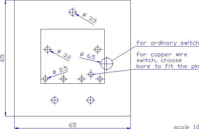
| Plexiglass cover: | Cut with a hacksaw, or grind a hook-like point to a knife, use this to make a carve in the plexiglass of about 1 mm deep, and then break it along the carve. | ||||
| 65 x 65 mm, ca. 3 mm thick, see fig. 5.8 | |||||
| Switch: |
|
A switch can be made of massive 0.75 mm² copper wire, see fig. 5.7 for size and shape. A more reliable solution is to buy a change-over push-button switch. Most push-button switches are single and have only 2 connections. Make sure to get one with 3 connections. | |||
| S | |||||
| Button: (for copper wire switch only) | Preferably the button should be plastic but wood or even metal (an M3 bolt) can be used. See fig. 5.6 and fig. 5.7 for the size and shape. Chips are often sold in tubes which are closed at both ends with plastic pins, these pins are perfect. | ||||
| ca. 6 mm long, 3 mm diameter | |||||
| Screws: | |||||
| M3 x 25 mm bolts, 2 pc. | |||||
| M3 nuts, 6 pc. | |||||
| wood screws, about 3 x 25 mm, 3 pc. | |||||
| Additional parts (only needed in special cases): | |||||
| Chip connector: | It is needed only for making test indicators where chips can be plugged in instead of soldered in, see annex D.5: Checking components. | ||||
| 18 pin dual-in-line. | |||||
| NTC resistor: | indifferent | Only needed for making indicators that
have to be accurate under a wide range of temperatures,
see annex D.4.8: Temperature stability. Please note: The temperature drift is caused by the LM3914 chip. An NTC of 22 Ohm would have improved temperature stability with all chips I have measured on. But chips from other production batches might need another NTC resistor for best temperature stability. |
|||
| 22 Ohm | |||||
Notes:
|
|||||
| 5.4.4.2 | Print lay-out and making the PCB |
There are several ways to make PCB's (Printed Circuit Boards). By far the most common way goes like this:
Finally the holes for the components are drilled and often the copper is covered with a protective layer against oxidation. Then the PCB is ready for fitting the components.
For unexperienced people, it seems a bit overcourageous to try producing PCB's in this way oneself right away. If the resulting PCB's would have a doubtfull quality, this could result in many more indicators that do not work because of poor soldering, tiny cracks in the copper strips etc. Finding these errors takes a lot of time and could be quite frustrating for unexperienced people. Also, for building PCB's this way, blank PCB material, several chemicals, a source of UV light and experience are needed. Workshops who sell these materials and can provide advice, might also produce PCB's according to design quite cheaply. Or a supply of ready-made PCB's can be bought from abroad (see par. 7.4).
In annex D.6: Making PCB's, a manual on how to produce PCB's in this way is given, together with simpler alternative ways which could be attractive in case no ready made PCB's can be bought and only small numbers are needed.
So now the problem of getting PCB's is reduced to finding a workshop who can make them, and providing them with a crystal-clear design.
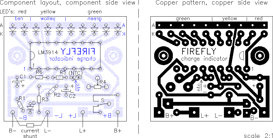
A print lay-out on scale 2:1 is given in fig. 5.4. Mind that the component lay-out is printed as seen from component side, while the copper pattern is printed as seen from copper side. That is why on the component lay-out drawing, the copper pattern appears in mirror image (see the blue, dotted areas and the thin lettering).
| |
| Fig. 5.4: Component layout and copper pattern of the Printed Circuit Board for the indicator. |
This lay-out is quite compact, it occupies a minium of space, is quite sturdy and consequently the PCB needs only 2 screws to fix it to the front cover. At the same time, this compactness leads to disadvantages: There is too little space for components if they happen to be larger than the standard ones and then some bending might be needed. Also the copper pattern is quite detailed and might be difficult to print properly in less well-equipped workshops.
The lay-out of fig. 5.4 shows the placing of the components that were included in the electrical circuit of fig. 5.3, and the copper pattern that is needed to connect them in the right way. There are `islands' onto which later the leads of components will be soldered, and there are copper strips that connect the islands.
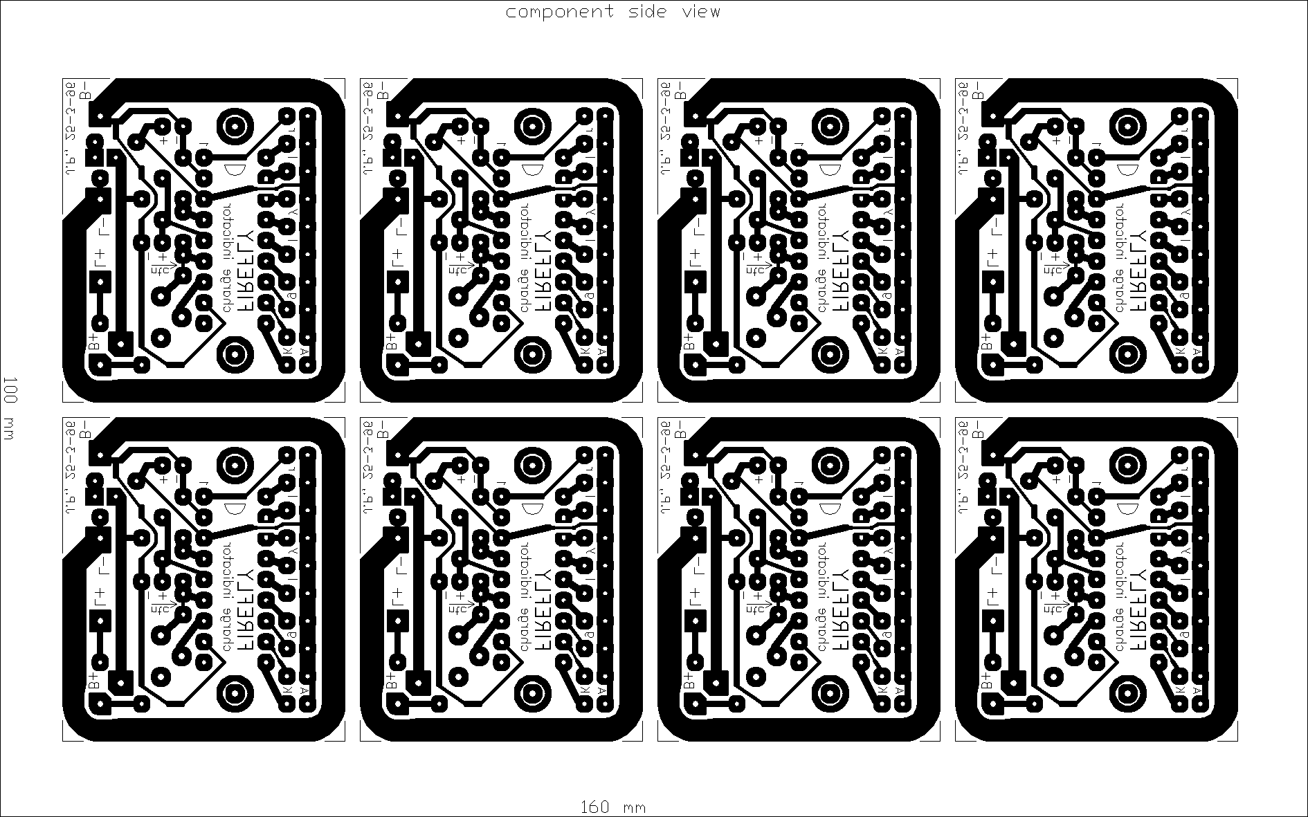
The coppern pattern of fig. 5.4 could be given to a workshop as a design for the PCB's. However, it is better to provide them with a transparant sheet that can be used directly. In fig. 5.5a, the same design is reduced to the correct size and 12 copies are placed on the smallest standard size PCB board. Here the copper pattern is printed in mirror image because it is best to have the transparant sheet in mirror image. Then the sheet can be laid on the blank PCB with the printed side facing down directly onto the light sensitive laquer and the clearest image will result. The copper pattern of fig. 5.5a can be copied directly onto thin tracing paper (the slightly transparant type of paper that is used for technical drawings) or transparant sheet with an ordinary copying machine. Please note that only special heat-resistant transparant sheet can be used in a copying machine, ordinary plastic will melt and make the copier jam. Check the quality of the copy carefully for:
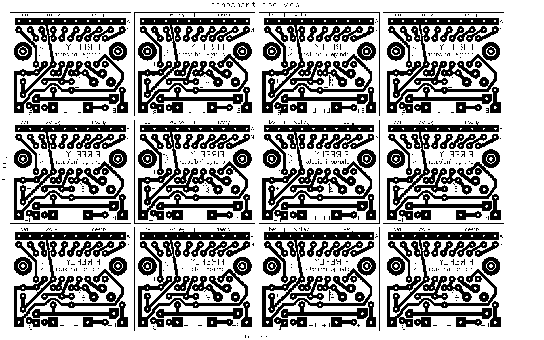 |
| Fig. 5.5a: Twelve copies of the PCB copper pattern (in
mirror image) fitted on standard size PCB board. Note: For correct dimensions, print this figure at 300 DPI (Dots Per Inch). |
 |
| Fig. 5.5b: Alternative: Eight copies of PCB design
with current shunt. Note: For correct dimensions, print this figure at 300 DPI (Dots Per Inch). |
If the tracing paper copy or transparant is O.K., it can be used directly by the workshop that will make the PCB's. There are many qualities of PCB material and if the workshop asks which one you prefer, choose for `epoxy' (colored white, slightly transparant) of ca. 1.0 mm thick. This is stronger and more resistant to humidity than the `pertinax' (light brown) that was used in older days. Especially the copper layer is fixed stronger on the base material and this reduces the risc that the iron wire that forms the switch will break loose. A disadvantage of epoxy is that it contains glass fibres that makes drill bits get blunt quite rapidly.
If the workshop will drill the holes, specify which holes have to be bored with what diameter, see below.
It makes sense to check the PCB's before accepting them, possible errors are:
After the pattern of fig. 5.5a is printed on PCB board, the 12 individual PCB's can be cut loose with a hacksaw and the holes must be drilled. Drilling is not difficult but when the workshop is willing to do this for a reasonable price, it saves a lot of work.
For drilling the holes, there are 3 options:
There are 4 kinds of `islands' on the copper pattern:
Clear copper will oxidize readily after it has been touched (the sweat from your fingers contains acids). A greenish-blue copper oxide layer will form and soldering later on will be more difficult. Of course the PCB's can be cleaned before soldering, but it is best to prevent oxidation by applying a protective layer on the PCB's before storing them. Electronic shops sell special sprays for this, but fixative (for charcoal drawings) will also do. Even grease or vaseline will do as long as it does not conduct electricity (check this with a tester on the highest resistance range).
Also after the indicators have been built, tested and calibrated, it makes sense to apply a protective layer on the PCB's. At least it will make them look better and make soldering easier when you would have to repair them.
| 5.4.4.3 | Fitting the components |
First a safety issue: A hot soldering iron has about the worst temperature with respect to creating burns. It is so hot that your skin will be severely burned before you feel the heat, while it is not hot and large enough to radiate so much heat that you will notice it before touching it. Therefor:
Fitting the components is not difficult. Basically, the work goes like this:
To work faster, one could stick a number of components onto the PCB, bend and cut all leads in one go, and then solder them. If several indicators are to be made, it is best to work on all of them at the same time, so fit the same component on all indicators and then fit the next component. Have the different resistors sorted into little boxes before starting to fit them. This also reduces the risc of misplacing components.
For resistor R1, R2, R5 and R6, the holes are drilled so close together that they do not fit when placed horizontally. So bend one lead 180° and fit these resistors vertically, see fig. 5.6. Make sure that the blank, upright leads do not make short-circuit with leads from other components.
For fitting the 10 LED's neatly on a row, a simple jig is a great help. This could be:
On the PCB, the LED's are placed 3.4 mm apart while the lower portion of some types of LED's have a diameter of up to 3.7 mm (the 3 mm size refers to the upper portion). With these LED's, file off a little from the lower portion until they fit properly besides one another.
For the soldering itself, there are also some point to pay attention to:
If an NTC resistor will be fitted to improve temperature stability, the PCB must be adapted. As printed, the two islands on the PCB onto which the NTC will be fitted, are connected by a narrow copper strip (the one where the `NTC' arrow points at in fig. 5.4). Only fitting an NTC will have no effect because it would be short-circuited by this narrow strip. So if an NTC is fitted, this narrow strip has to be cut, e.g. with a sharp knife. Check with a tester whether the two islands are really not connected any more.
If an NTC is fitted after calibration, the indicator must be calibrated again.
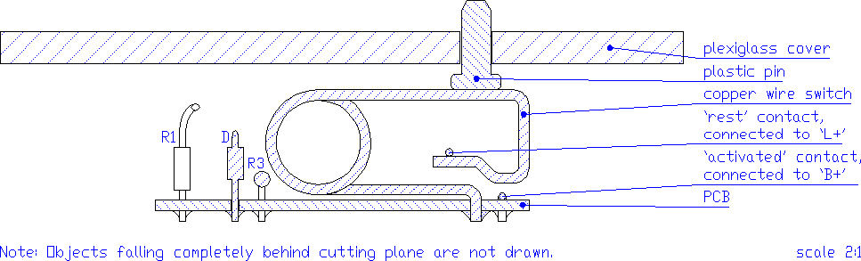
If no ready made push-button switch is used, switch S can be made from 0.75 mm² copper wire (ca. 1 mm diameter). The shape of the wire that forms the switch is drawn in fig. 5.7. See fig. 5.6 for how it looks in practice.
|
|
| Fig. 5.7: Cross section through copper wire switch. |
The wire that forms the switch, will be soldered to the PCB and there is a risc that when large forces are exerted on the iron wire, the copper layer will break loose from the base material of the PCB (therefor epoxy PCB material is preferable above pertinax, since with epoxy the copper layer is fixed better onto the base material). Once this has happened, it will be very difficult to repair. To minimise these forces, the iron wire should be bent to the proper shape before soldering it on the PCB, so that after soldering, no more bending is needed. Bending forces during normal use are minimal because the button is placed right above the point where the iron wire is fixed on the PCB.
The two contacts of the switch are just pieces of wire (e.g. excess length of leads of other electronic parts) that are soldered onto the proper islands. The one connected to `B+' is bent flat over the PCB. So when the copper wire is pushed down, it will touch this contact. The one connected to `L+' is bent to form a hook and touches the copper wire switch when it is not pushed downwards, see fig. 5.7.
Check whether the switch can not touch a metal part of trimmer R4 in any possible way.
A copper wire switch probably won't be too reliable because it is likely to oxidize under humid conditions. To reduce chances of problems, apply some solder on the contact surfaces. Grease would also help, but that will attract dust and then the dust could cause bad contacts. So this only makes sense if finished indicators are packed properly until they are fitted in their housing.
If a ready-made switch is used, the wires coming from the connector block could go directly to the switch, with the `L+' wire going to the connection that is normally `on' and the `B+' wire to the connection that is `on' when the switch is activated. Then the middle connection of the switch must be connected to the island where normally the copper wire switch is fitted. So then on the PCB, the islands for the `L+' and `B+' connections, and the islands where the contacts for the copper wire switch are fitted, remain unused.
Once the current shunt is fitted and wound up to a neat roll, the copper side of the PCB is inaccessible for testing or repair. Therefor it makes sense to first check whether indicators function (see par. 5.4.5) before fitting the current shunt. Without a current shunt, the indicator can't work so then the `B-' and `L-' connection must be short-circuited with a piece of wire.
Addition to internet version: PCB with on-board current shuntInstead of making a current shunt from copper wire, one could also use the PCB design of fig. 5.5b with an on-board current shunt. With this PCB design, there is a copper strip between `B-' and `L-' that has such a length and width that its resistance is ca. 0.02 Ohm. Of course also thickness of this copper strip plays a role, so it can only be used with PCB material with the usual 0.035 mm copper layer. When in doubt: Check resistance afterwards by having a stable DC current going through it (e.g. from a lamp connected to a battery) and measuring voltage drop over the shunt with a digital tester on mV DC range.
As stated in the parts list, the current shunt consists of 860 mm of 0.75 mm² copper wire. Start with a length of ca. 940 mm, strip off ca. 42 mm of the isolation on both ends and stick the ends through the PCB from the copper side. Bend the long current shunt in a neat way behind the PCB so that it doesn't occupy too much space. Then solder it to the PCB. Now the ends stick through at the component side and a length of isolation can be shoved onto them again. These protruting ends can be used to connect the indicator to the connector block.
To limit the power consumption of the indicator, the LED current is kept to a minimum and consequently the LED's light up only dimly. To make the LED's look brighter, wrap some black electrical tape around the row of LED's. This will prevent ambient light from entering LED's from the side. Then LED's that are off, will look darker and the one that is on, is more conspicious.
The plexiglass cover provides no complete housing for the indicator. It only forms a basis onto which the other parts can be fitted and because it is transparant, the LED's behind it, remain visible. Users themselves could make the rest of the housing using woodcarving: A piece of wood with a space carved out that is large enough for the indicator to fit in. The plexiglass cover with indicator itself mounted on the back, can be fitted onto this piece of wood.
|
|
| Fig. 5.8: A plexiglass cover. |